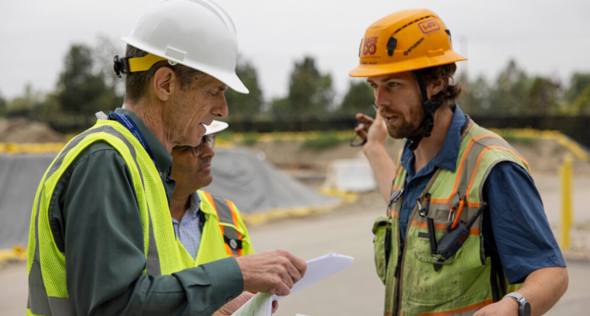
ALBANY, N.Y. — New York State leaders marked a major milestone Monday as ironworkers raised the final steel beam into place for NanoFab Reflection, the newest building rising at the expanding Albany NanoTech complex. The ceremonial topping-off celebrated the rapid progress on what officials describe as one of the most important semiconductor research facilities ever built in the United States.
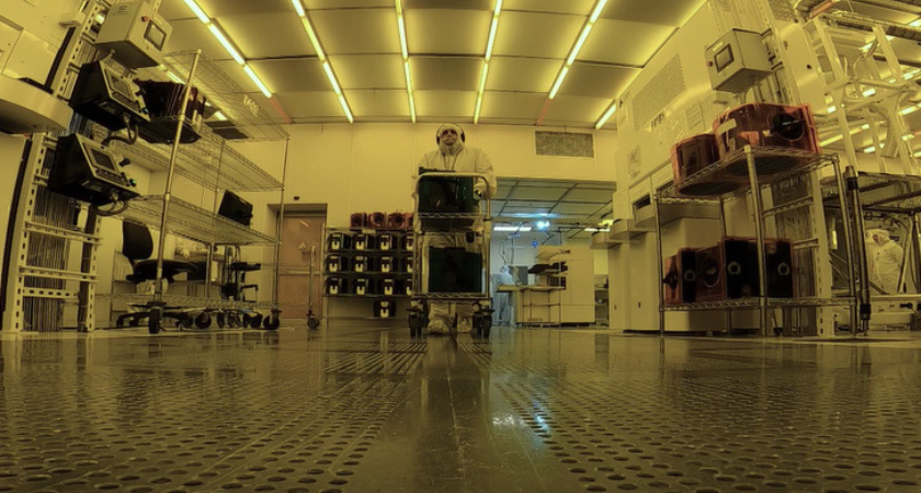
NanoFab Reflection will house the nation’s first publicly owned High NA EUV Lithography Center, where the world’s most advanced lithography equipment will be used to print the ultra-small features essential for next-generation computer chips. The technology is considered the defining tool for the next era of semiconductor innovation, allowing researchers and manufacturers to prototype and develop chips that are smaller, faster, and more powerful than any created today. State and industry officials say the building positions Albany to serve as a global hub for high-end chip development.
The project also reflects New York’s broader strategy to strengthen its semiconductor ecosystem—a sector that continues to expand rapidly through research investment, manufacturing announcements, and workforce development partnerships. As the beam was raised, leaders emphasized that the impact of NanoFab Reflection will extend far beyond the construction site itself.
“I want more of those jobs created in the building of these facilities. We’re seeing that all over now but also what happens inside these building,” Gov. Kathy Hochul said. “This will be home to North America’s premier lab for semiconductor research right here in Albany. The most elite, smartest people are going to be congregating here, and I think that’s just extraordinary.”
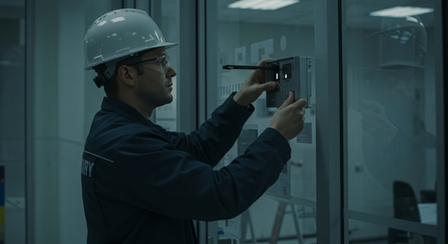
State officials expect the facility to generate hundreds of new high-tech research and engineering jobs, with ripple effects across academic institutions, supply chain companies, and training programs preparing the next generation of chip specialists. They also estimate that the project will help attract $9 billion in private investment, expanding partnerships with universities and major semiconductor companies that rely on cutting-edge lithography research.
Construction of NanoFab Reflection is expected to be completed by late 2026, at which point it will serve as the centerpiece of New York’s growing semiconductor corridor—an anchor for innovation, workforce development, and global industry collaboration. With Monday’s milestone, the project moves into its next phase of interior and systems work, bringing the state one step closer to operating what leaders are calling the world’s most advanced chip R&D center.
Originally reported by Sydney Havens in News 10.Com